
[2021-09-24] Ten Lessons From Three Generations Shaped Google’s TPUv4i : Industrial Product
Published:
I was quite busy during this year’s ISCA, so I did not have the chance to read the papers or watch the videos carefully. I will try to read the ISCA 2021 papers that I am interested in, hopefull before MICRO 2021 starts.
This paper is a industry-track paper that is written by the Google TPU team. This paper views TPU genrations and learns lessions from it in the perspective of industry, which is quite interesting and gives me more industry insights.
Ten lessons
- Logic,wires,SRAM,& DRAM improves unequally:
- Wires, SRAM has smaller gains when scling from 45nm to 7nm.
- Logic improves much faster than wires and SRAM, so logic is relatively “free”, like HBM.
- Leverage prior compiler optimizations
- TPU use XLA (Accelerated Linear Algebra) compiler
- Design for performane per TCO vs per CapEx
- Captical Expense (CapEx) is the price for an item
- Operation Expense (OpEx) is the cost of operation
- TCO = CapEx + 3 * OpEx
- Support backward ML compatibility
- Inference DSAs need air cooling for global scale
- Some inference apps need floatin point arithmetic
- ML acclerator usually use quantized models for inference to save area and power while using fp for training
- But some apps like segmentation don’t work well when quantized
- In TPUv1, app developers said 1\% acc drop is acceptable, but DNN overall quality improved so 1\% is large.
- Production inference normally needs multi-tenancy
- Sharing can lower cost and reduce latency
- Support multiple batch sizes to balance throughput and latency
- need fast switching time between models, so DSAs need local memory
- I am curious about the security issues for sharing hardware for different apps. How to isolate them?
- DNNs grow ~1.5x/year in memory and compute
- DNN workloads evolve with DNN breakthroughs
- Inference SLO(Service Level Objectives) limit is P99 latency, not batch size
TPUv4i
The block diagram is shown below. 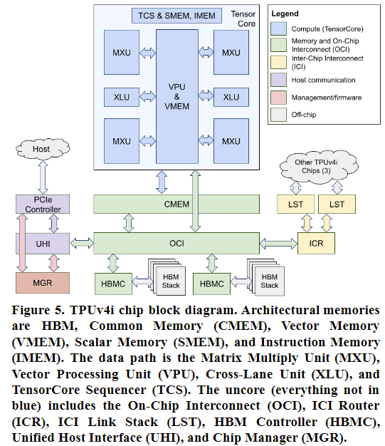
- A single-core chip for inference (like TPUv1) and a dual-core chip for training (like TPUv3)
- Be compiler compatible rather than binary compatible; XLA produces High Level Operations (HLO) that are machine indepedent and Low-Level Operations (LLO) that are machine dependent.
- Increase on-chip SRAM storage with common memory (CMEM); choose 128MB.
- DMA engines distrbiuted throughout the chip’s uncore to mitigate interconnect latency and wire scaling challenges; 4D tensor DMA supports arbitrary steps-per-stride and positive/negative stride distances in each dimension. (I do not quite understand the meaning of 4D here)
- Supports bf16 and int8, so quantization is optional
Performance
TPUv4i has similar performance with TPUv3, but it has better perf/TCO at 2.3x vs TPUv3.